Photolithography
Background: I was planning to synthesize the micro-structure as the skeleton for the growth of the nano-roughness feature. This design is conventionally adopted to avoid the failure of the self-propelling mechanism.
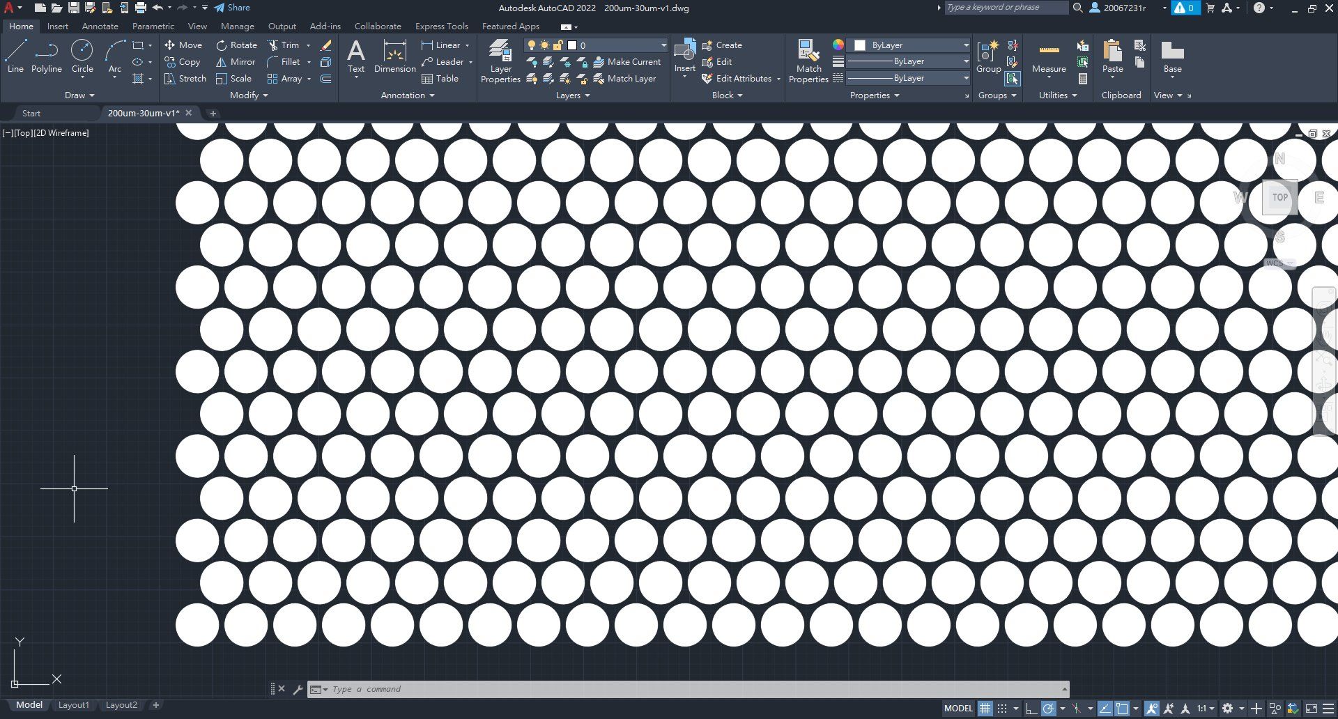
To begin with, I designed the mask on AutoCad (Figure 1). Then I sent the drawing to the commercial company to synthesize it.
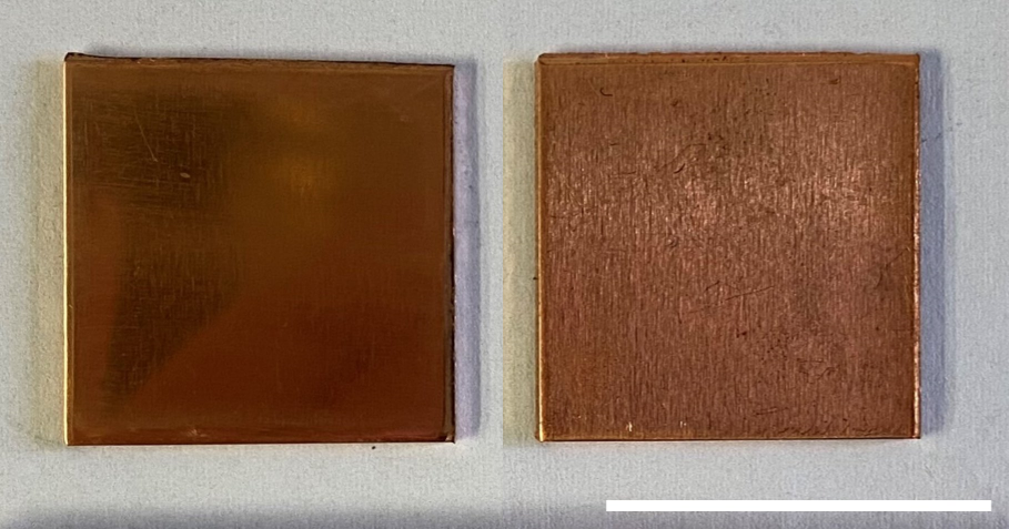
Before the photolithography, I polished the copper to remove the oxide and organic contaminants by abrasion with #5000 sandpaper. After the abrasion, we can see the luster and clean surface (Figure 2). This step ensures success in photoresist deposition.
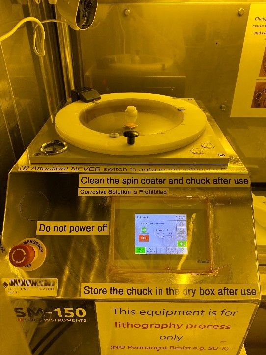
The polished copper was placed into the spin-coater (Figure 3). The vacuum pump provides the pressure difference to fix the copper. However, my copper substrate is too heavy. Therefore, I made some trial and error to find the position where the center of mass of the copper had minimum displacement during the spin-coating.
I tried AZ5214E and AZ9260 to coat the copper, and both performed good protection performance in the following treatment. Therefore, I had chosen the AZ5214E because our clean room has a better supply. After the spin-coating, the coated copper was placed on the hotplate to conduct soft-bake, where the photoresist was solidified.
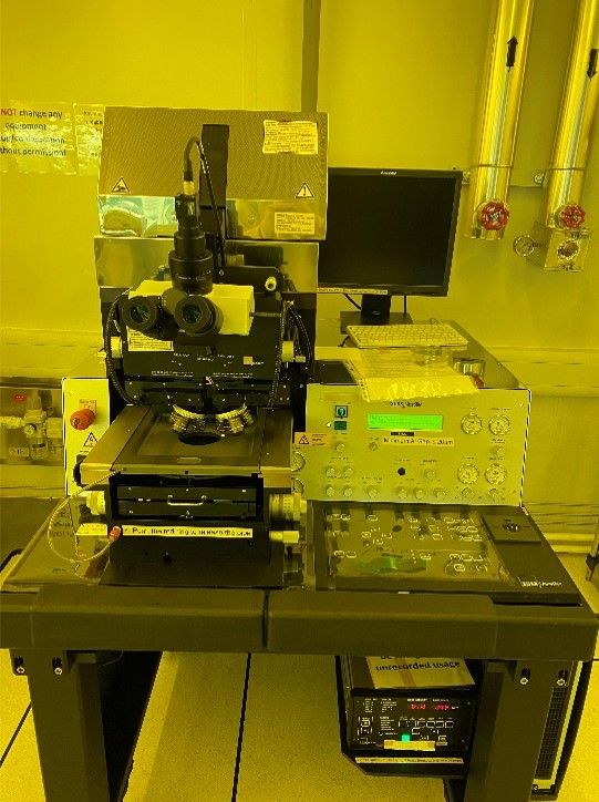
Then the coated copper was placed inside the Suss MA6 Aligner to conduct exposure (Figure 4). After the exposure, the develop process was carried out by immersed the sample into the AZ300 MIF, where the exposed photoresist will be removed.
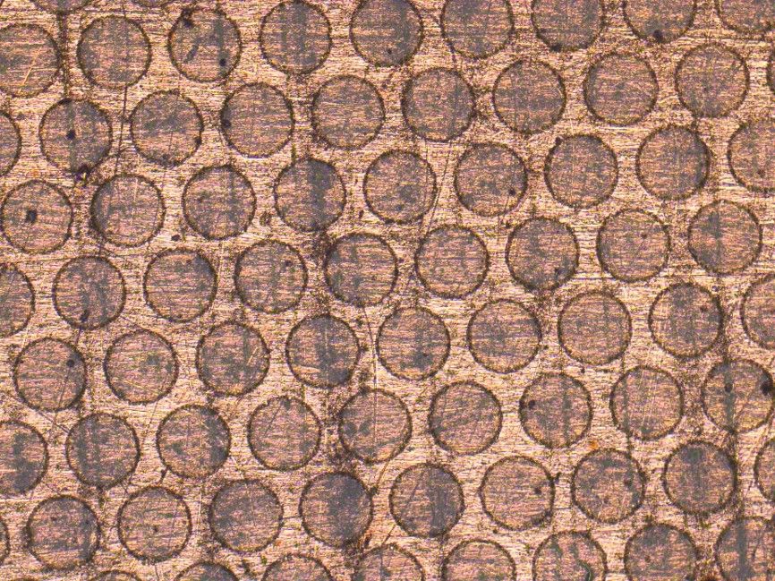
It is easy to examine the above process with Optical Microscope (Figure 5). If everything was correct, we can see the image that two different contrast form the matrix pattern. Finally, I placed the sample inside the copper etchant to etch away the unprotected area.
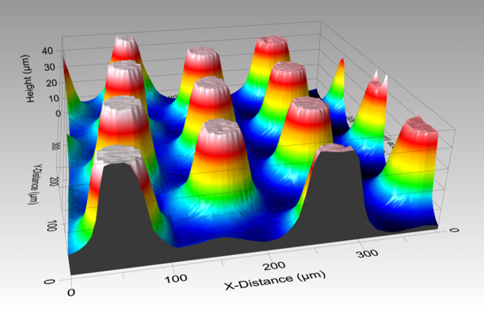
After the copper ecthing and lift-off process, I examine the sample with 3D mapping (Figure 6).